- 您现在的位置:买卖IC网 > Sheet目录3886 > PIC16C54C-04/SO (Microchip Technology)IC MCU OTP 512X12 18SOIC
PIC18F2450/4450
2006 Microchip Technology Inc.
Advance Information
DS39760A-page 61
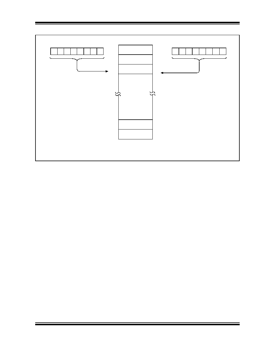
FIGURE 5-6:
USE OF THE BANK SELECT REGISTER (DIRECT ADDRESSING)
5.3.3
ACCESS BANK
While the use of the BSR, with an embedded 8-bit
address, allows users to address the entire range of
data memory, it also means that the user must always
ensure that the correct bank is selected. Otherwise,
data may be read from or written to the wrong location.
This can be disastrous if a GPR is the intended target
of an operation but an SFR is written to instead.
Verifying and/or changing the BSR for each read or
write to data memory can become very inefficient.
To streamline access for the most commonly used data
memory locations, the data memory is configured with
an Access Bank, which allows users to access a
mapped block of memory without specifying a BSR.
The Access Bank consists of the first 96 bytes of
memory (00h-5Fh) in Bank 0 and the last 160 bytes of
memory (60h-FFh) in Block 15. The lower half is known
as the “Access RAM” and is composed of GPRs. The
upper half is where the device’s SFRs are mapped.
These two areas are mapped contiguously in the
Access Bank and can be addressed in a linear fashion
by an 8-bit address (Figure 5-5).
The Access Bank is used by core PIC18 instructions
that include the Access RAM bit (the ‘a’ parameter in
the instruction). When ‘a’ is equal to ‘1’, the instruction
uses the BSR and the 8-bit address included in the
opcode for the data memory address. When ‘a’ is ‘0’,
however, the instruction is forced to use the Access
Bank address map; the current value of the BSR is
ignored entirely.
Using this “forced” addressing allows the instruction to
operate on a data address in a single cycle without
updating the BSR first. For 8-bit addresses of 60h and
above, this means that users can evaluate and operate
on SFRs more efficiently. The Access RAM below 60h
is a good place for data values that the user might need
to access rapidly, such as immediate computational
results or common program variables. Access RAM
also allows for faster and more code efficient context
saving and switching of variables.
The mapping of the Access Bank is slightly different
when the extended instruction set is enabled (XINST
Configuration bit = 1). This is discussed in more detail
5.3.4
GENERAL PURPOSE
REGISTER FILE
PIC18 devices may have banked memory in the GPR
area. This is data RAM which is available for use by all
instructions. GPRs start at the bottom of Bank 0
(address 000h) and grow upwards towards the bottom of
the SFR area. GPRs are not initialized by a Power-on
Reset and are unchanged on all other Resets.
Note
1:
The Access RAM bit of the instruction can be used to force an override of the selected bank (BSR<3:0>) to
the registers of the Access Bank.
2:
The MOVFF instruction embeds the entire 12-bit address in the instruction.
Data Memory
Bank Select(2)
7
0
From Opcode(2)
000
0
000h
100h
200h
300h
F00h
E00h
FFFh
Bank 0
Bank 1
Bank 2
Bank 14
Bank 15
00h
FFh
00h
FFh
00h
FFh
00h
FFh
00h
FFh
00h
FFh
Bank 3
through
Bank 13
00
1
111
7
0
BSR(1)
发布紧急采购,3分钟左右您将得到回复。
相关PDF资料
PIC16F722-I/ML
IC PIC MCU FLASH 2KX14 28-QFN
PIC16LCE623T-04I/SO
IC MCU CMOS.5K OTP W/EEPRM18SOIC
PIC16HV540-04I/SO
IC MCU OTP 512X12 18SOIC
PIC16LCE623T-04E/SS
IC MCU CMOS.5K OTP W/EEPRM20SSOP
PIC16LCE623T-04E/SO
IC MCU CMOS.5K OTP W/EEPRM18SOIC
5-520415-4
CONN TRIOMATE 4POS VERT TIN
6-176982-6
CONN TRIO-MATE 16POS .100 FFC
PIC16LCE623-04I/SO
IC MCU CMOS.5K OTP W/EEPRM18SOIC
相关代理商/技术参数
PIC16C54C-04/SO
制造商:Microchip Technology Inc 功能描述:8BIT CMOS MCU SMD 16C54 SOIC18
PIC16C54C-04/SO
制造商:Microchip Technology Inc 功能描述:Microcontroller IC Number of I/Os:12
PIC16C54C-04/SS
功能描述:8位微控制器 -MCU .75KB 25 RAM 12 I/O 4MHz SSOP20 RoHS:否 制造商:Silicon Labs 核心:8051 处理器系列:C8051F39x 数据总线宽度:8 bit 最大时钟频率:50 MHz 程序存储器大小:16 KB 数据 RAM 大小:1 KB 片上 ADC:Yes 工作电源电压:1.8 V to 3.6 V 工作温度范围:- 40 C to + 105 C 封装 / 箱体:QFN-20 安装风格:SMD/SMT
PIC16C54C-04E/P
功能描述:8位微控制器 -MCU .75KB 25 RAM 12 I/O 4MHz ExtTemp PDIP18 RoHS:否 制造商:Silicon Labs 核心:8051 处理器系列:C8051F39x 数据总线宽度:8 bit 最大时钟频率:50 MHz 程序存储器大小:16 KB 数据 RAM 大小:1 KB 片上 ADC:Yes 工作电源电压:1.8 V to 3.6 V 工作温度范围:- 40 C to + 105 C 封装 / 箱体:QFN-20 安装风格:SMD/SMT
PIC16C54C-04E/SO
功能描述:8位微控制器 -MCU .75KB 25 RAM 12 I/O 4MHz Ext Temp SOIC18 RoHS:否 制造商:Silicon Labs 核心:8051 处理器系列:C8051F39x 数据总线宽度:8 bit 最大时钟频率:50 MHz 程序存储器大小:16 KB 数据 RAM 大小:1 KB 片上 ADC:Yes 工作电源电压:1.8 V to 3.6 V 工作温度范围:- 40 C to + 105 C 封装 / 箱体:QFN-20 安装风格:SMD/SMT
PIC16C54C-04E/SS
功能描述:8位微控制器 -MCU .75KB 25 RAM 12 I/O 4MHz Ext Temp SSOP20 RoHS:否 制造商:Silicon Labs 核心:8051 处理器系列:C8051F39x 数据总线宽度:8 bit 最大时钟频率:50 MHz 程序存储器大小:16 KB 数据 RAM 大小:1 KB 片上 ADC:Yes 工作电源电压:1.8 V to 3.6 V 工作温度范围:- 40 C to + 105 C 封装 / 箱体:QFN-20 安装风格:SMD/SMT
PIC16C54C-04I/P
功能描述:8位微控制器 -MCU .75KB 25 RAM 12 I/O 4MHz IndTemp PDIP18 RoHS:否 制造商:Silicon Labs 核心:8051 处理器系列:C8051F39x 数据总线宽度:8 bit 最大时钟频率:50 MHz 程序存储器大小:16 KB 数据 RAM 大小:1 KB 片上 ADC:Yes 工作电源电压:1.8 V to 3.6 V 工作温度范围:- 40 C to + 105 C 封装 / 箱体:QFN-20 安装风格:SMD/SMT
PIC16C54C-04I/P
制造商:Microchip Technology Inc 功能描述:IC 8BIT CMOS MCU 16C54 DIP18